
Fully Automatic Wafer Debonder
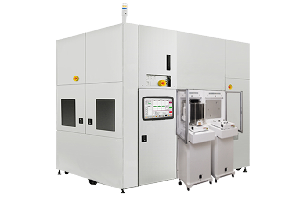
4"-8"/ 8"-12"wafer application.
Thinner wafer capability
Compatible wafer cassette /wafer box
Used bonding tape robot peeling
Automatic wafer mounting
Built-in UV irradiating module
PC based control with Windows OS
Intelligent wafer mapping in cassette
SECS/GEM or simple link capability
Automatic bonded wafer aligning
Thermal debonding device wafer & support wafer
For more information, Please contact us.
building 6, Nanfang Urban Park, Lane 1165, Jindu Road, Minhang District, Shanghai,China.
302, 3rd Floor, Building B, Kaicheng High tech Park, Dalang Street, Longhua District, Shenzhen, China